
Let me describe a scenario I have seen more than once. A federal program office spends eighteen months achieving FedRAMP High authorization for its AI platform. The infrastructure runs inside a GovCloud enclave. The data never leaves U.S. soil. The cryptographic modules carry FIPS 140-3 validation certificates. Every compliance box is checked. And 100% of the inference silicon powering that platform was designed in one country, fabricated in another, packaged and tested in a third, and shipped across the Pacific on a four-to-six-week logistics timeline that a single geopolitical disruption could sever. Stop and think about that for a moment. We have built an entire “sovereign AI” conversation around model weights, data residency, and inference locality, and that conversation is necessary but dangerously incomplete. Sovereignty is not just about where the data sits or who controls the model. It is about who controls the physical substrate that makes inference possible in the first place, i.e., the silicon, the package, the test floor, and the supply chain that connects them.
Date
05.12.2026
Author
Shailesh Patel
The Blind Spot in Sovereign AI
The term "sovereign AI" has become a fixture in policy circles, enterprise boardrooms, and defense acquisition strategies over the past two years. When most people use it, they mean one or more of the following: the AI model was trained on domestically governed data, the model weights are controlled by a domestic entity, and inference runs on infrastructure inside national borders. These are all legitimate dimensions of sovereignty. But they describe sovereignty at the software and data layer while ignoring the hardware layer entirely.
Here is the question that rarely gets asked: where was the chip fabricated? Where was it packaged? Where was it tested? And if the answer to all three is "somewhere in East Asia," then what exactly is sovereign about the compute?
FIPS 140-3 validates that a cryptographic module meets specific security requirements. It says nothing about where the silicon in that module was manufactured, assembled, or tested. FedRAMP authorizes a cloud service provider's infrastructure against NIST SP 800-53 controls. It says nothing about the geographic origin of the processors inside that infrastructure. These frameworks solve the problems they were designed to solve, and they solve them well. But they were not designed to address supply chain provenance at the substrate level, and we should stop pretending that compliance with them constitutes sovereignty over the compute layer.
The Numbers Tell the Story
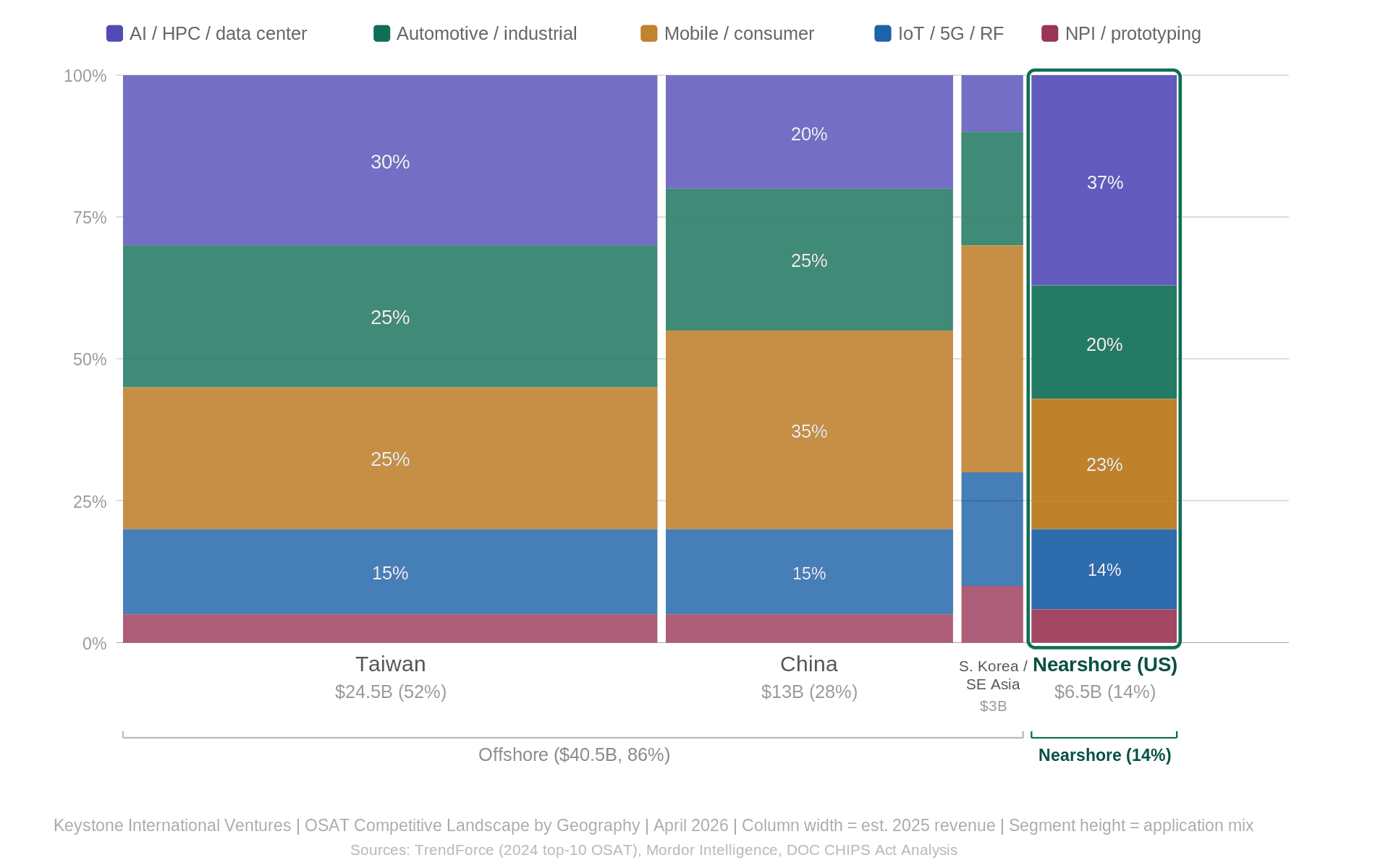
Let me put this in perspective. As of 2024, the top ten Outsourced Semiconductor Assembly and Test (i.e., OSAT) companies generated $41.56 billion in combined revenue.
ASE, headquartered in Taiwan, holds roughly 45% of that market. Amkor, the sole U.S.-headquartered company in the top three, holds 15.2%. JCET, based in China, holds 12% and posted 19.3% year-over-year growth. The remaining top ten positions are held by companies in China, Taiwan, South Korea, and Singapore.
The geographic picture is even starker. Depending on whose numbers you use, Asia-Pacific accounts for somewhere between 73% and 81% of global OSAT capacity. The U.S. Department of Commerce, in its own CHIPS Act analysis, cited 81% of global OSAT capacity located in East Asia, with 38% in China alone. That means the back end of the semiconductor value chain (i.e., the assembly, packaging, and testing that turn a bare die into a functional chip) is overwhelmingly concentrated in a region subject to escalating geopolitical risk, trade restrictions, and logistics fragility.
When we talk about "reshoring" semiconductor manufacturing, we tend to focus on the fab. TSMC is building in Arizona. Intel is expanding in Ohio. Samsung is investing in Texas. These are significant and necessary investments. But a chip is not a product when it leaves the fab. It is a product when it leaves the OSAT, packaged, tested, and ready for integration into a system. If the back end of the value chain remains offshore, then reshoring the front end is necessary but not sufficient.
CHIPS Act: Progress and Gaps
The CHIPS and Science Act of 2022 represent the most significant U.S. semiconductor industrial policy in a generation. The National Advanced Packaging Manufacturing Program (NAPMP) has awarded $1.4 billion specifically aimed at developing advanced packaging technologies and building a domestic end-to-end ecosystem. An additional $300 million went to the NIST Advanced Packaging Manufacturing Program for substrate chemistry research, and $200 million funded a Manufacturing USA Institute focused on digital twins in semiconductor design.
These are real investments, and they matter. But context is important. The global OSAT market is projected to reach $77 billion by 2031. The entire NAPMP allocation, spread across research, prototyping, and pilot production, represents less than 2% of that figure. The CHIPS Act is a down payment on packaging sovereignty, not the full purchase price. Closing the gap will require sustained investment, commercial demand signals, and a policy environment that makes domestic and nearshore OSAT operations economically viable over the long term.
The Section 232 tariff proclamation of January 2026 added another dimension. The initial 25% tariff is narrowly targeted at high-performance AI processors, but the proclamation directs the Secretary of Commerce to recommend broader semiconductor tariffs by July 2026, with a tariff offset program for companies investing in domestic production. This is the policy machinery beginning to address the back-end concentration problem, but the offset program's design will determine whether it accelerates domestic OSAT investment or simply increases costs for downstream consumers without moving capacity.
Two Kinds of Sovereignty
I find it useful to distinguish between two layers of sovereignty that get conflated in most discussions.
The first is cryptographic and compliance sovereignty. This is the layer addressed by FIPS 140-3, FedRAMP, FISMA, and the NIST SP 800-53 control families. It ensures that data is encrypted with validated modules, that infrastructure meets defined security baselines, and that operations are governed by auditable controls. This layer is mature, well-understood, and enforceable. It is also where most of the federal "sovereign AI" conversation lives today.
The second is substrate sovereignty. This is the layer that asks: who controls the physical components that make the compute possible? Where are the wafers fabricated? Where are the dies cut, packaged, wire-bonded or flip-chipped, encapsulated, and tested? What is the logistics timeline from package to deployment, and how many national borders does a chip cross before it reaches a U.S. data center or edge device? This layer is poorly defined, rarely measured, and largely unaddressed by existing compliance frameworks.
Cryptographic sovereignty without substrate sovereignty is a contradiction. You can validate every cryptographic module in your stack, and if the silicon supply chain runs through a single chokepoint 8,000 miles away, you have a sovereignty gap that no FedRAMP authorization can close.
What This Means for CTOs
If you are a federal CTO or a CISO building an AI capability, I am not suggesting you need to source every chip domestically tomorrow. The supply chain does not support that, and pretending otherwise is not useful. But I am suggesting three things worth thinking about.
First, know your supply chain deeper than the cloud provider. When you sign a GovCloud contract, you inherit a silicon supply chain you probably have not mapped. Ask the question. Your cloud provider's AI accelerators were fabricated, packaged, and tested somewhere. You should know where.
Second, watch the CHIPS Act Phase 2 investments in packaging and test, not just in fabs. The fab investments get the headlines. The packaging investments are where the supply chain diversification actually happens. If nearshore OSAT capacity materializes in North America (i.e., leveraging USMCA trade advantages, shared time zones, and 4 to 5-day logistics instead of 4-6 weeks), that is a structural shift worth understanding.
Third, start distinguishing between cryptographic sovereignty and substrate sovereignty in your own architecture documentation. Your SSP addresses the first. Nothing in your current compliance stack addresses the second. That gap is worth naming, even if closing it takes years.
This is the beginning of a longer conversation. In two weeks, I will unpack why the center of gravity in AI is shifting from hyperscale training to distributed edge inference, and why performance per watt at the edge is the metric that will define which AI applications are economically viable. The substrate question only gets harder when the chip has to run in a 50-watt enclosure on a mine haul truck instead of a climate-controlled data center.
The silicon matters as much as the model. We should start acting like it.
This is the first in a series on AI infrastructure, federal AI governance, and delivery methodology. Next: "Edge Inference Is the Real AI Infrastructure Story" (May 4, 2026).
Shailesh Patel is CTO of Keystone International Ventures and a SAFe Program Consultant (SPC). He writes about the intersection of AI architecture, federal technology, and the delivery frameworks that connect them.